back back

—Class D Amplifier

I designed and built a Class-D Amplifier with a discrete driver stage to explore analog signal processing and the basics of audio amplification.

Tools: Altium Designer, LTSpice, Oscilloscope

Keywords: switching amplifer, filter design, digital logic, analog amplification

Class-D Amplifier Prototype

—Starting Point

As a music lover, I thought that it would be a fun project because it combines analog and digital circuitry to create a relatively efficient speaker.

I started with a block diagram for a standard class-d amplifier:
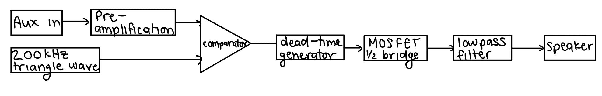
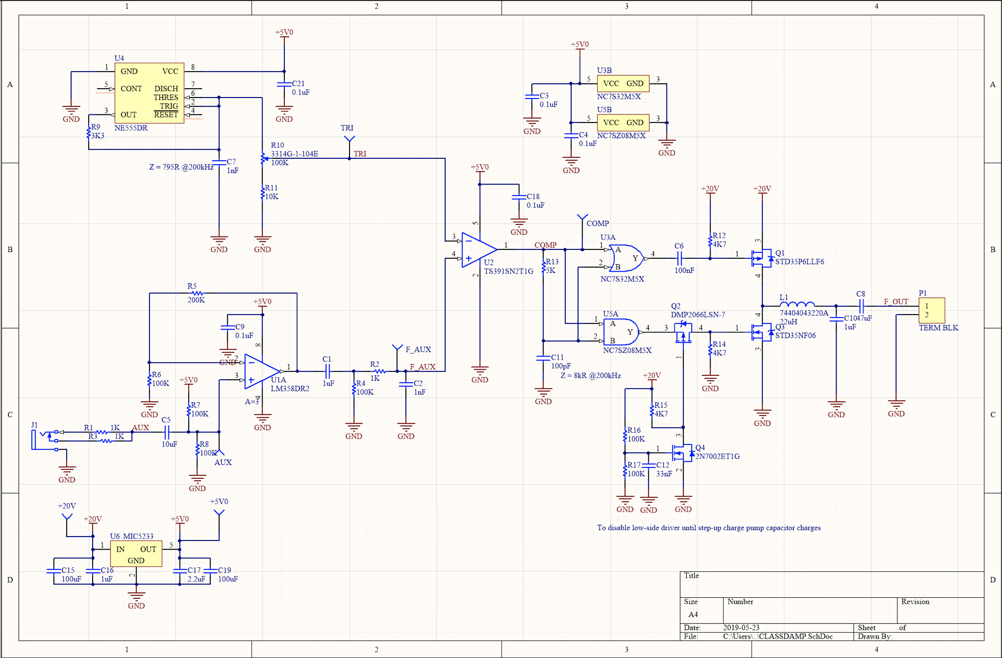
Some notes

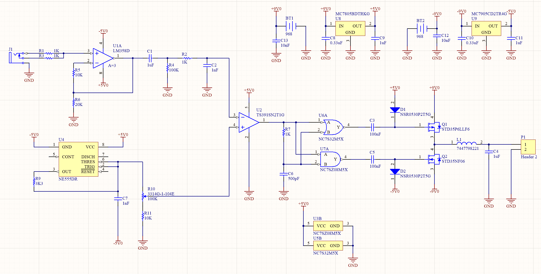
Aux in: The signal (when measured) was around 60mV.

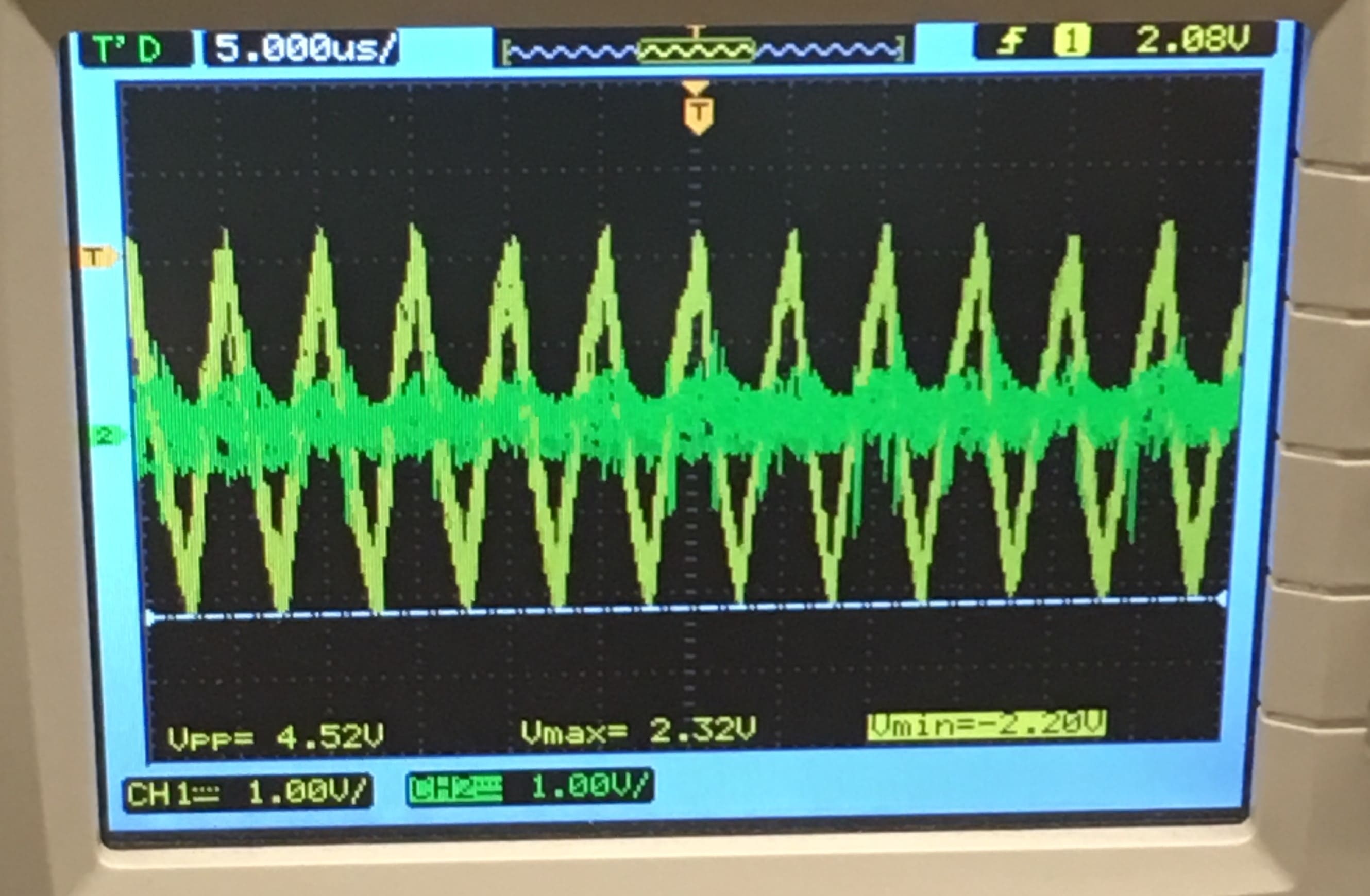
200kHz triangle wave: 200kHz is 10x the upper limit of human hearing, so the sound quality will be maintained when the audio signal is encoded as a time-varying PWM signal.

Comparator: Propagation delays of the selected component need to be much lower than 5us (the frequency of the triangle wave)

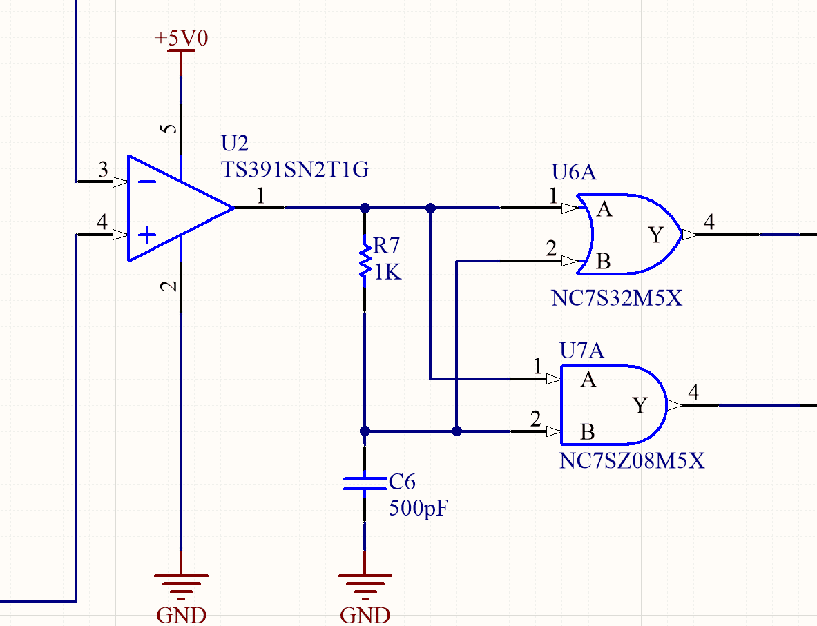
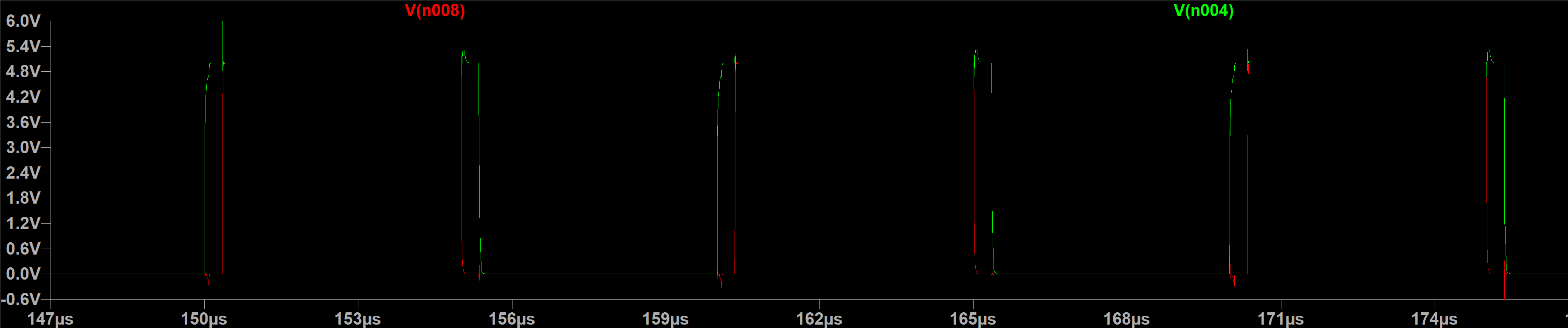
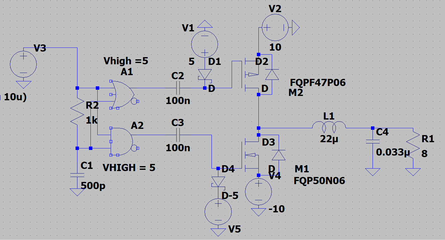
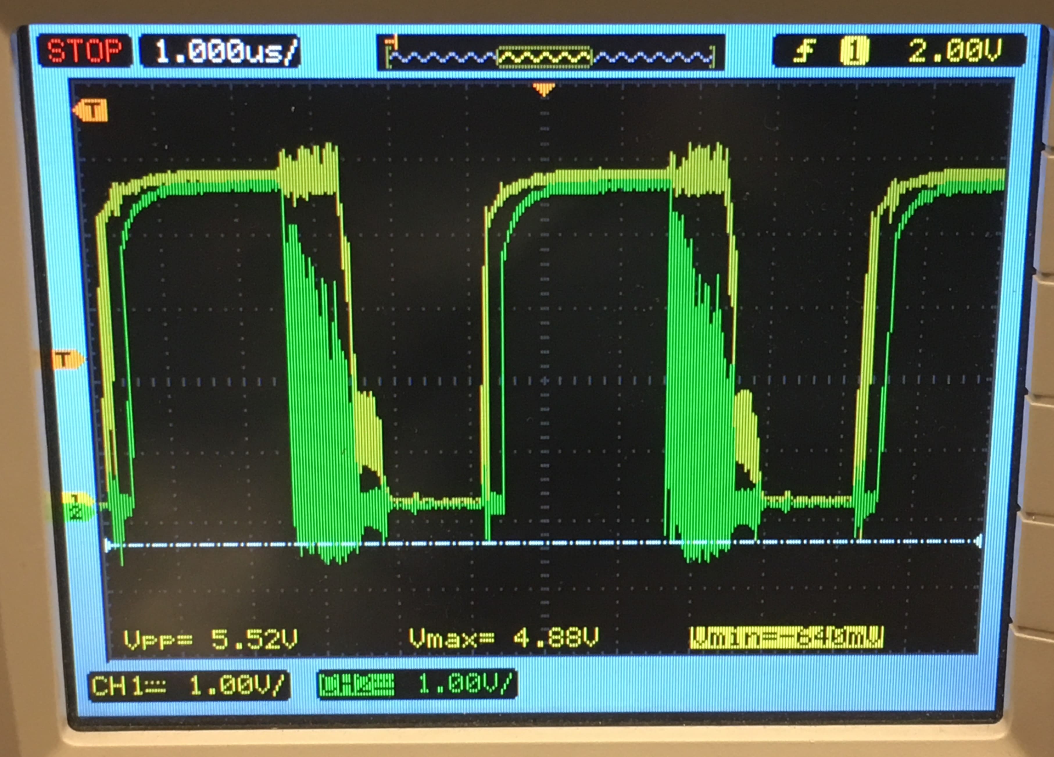
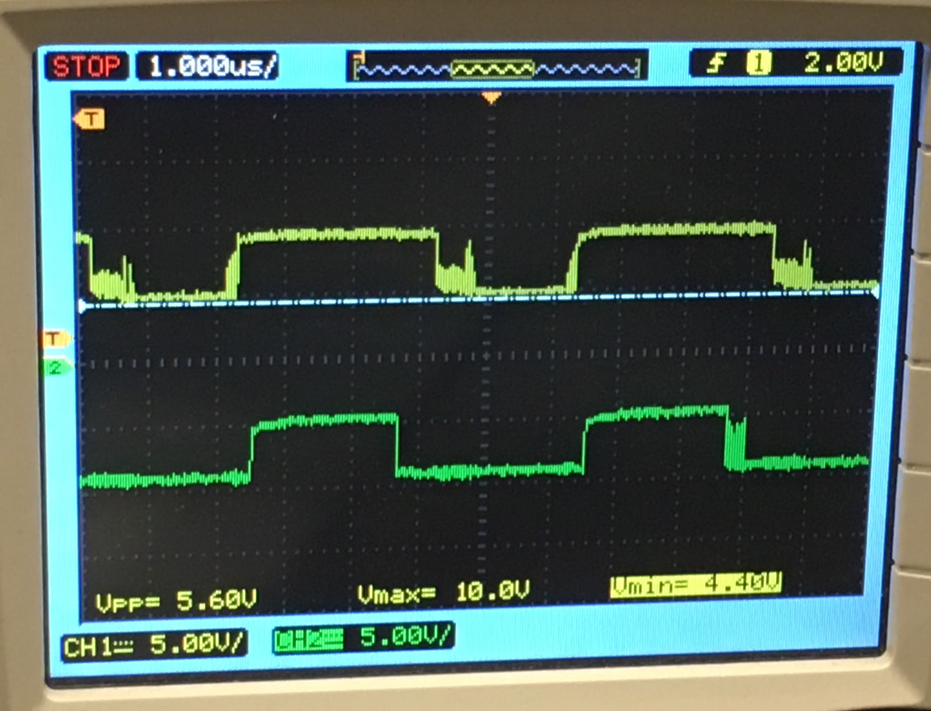
Dead-time generator: The high-side and low-side MOSFETs cannot be on at the same time.

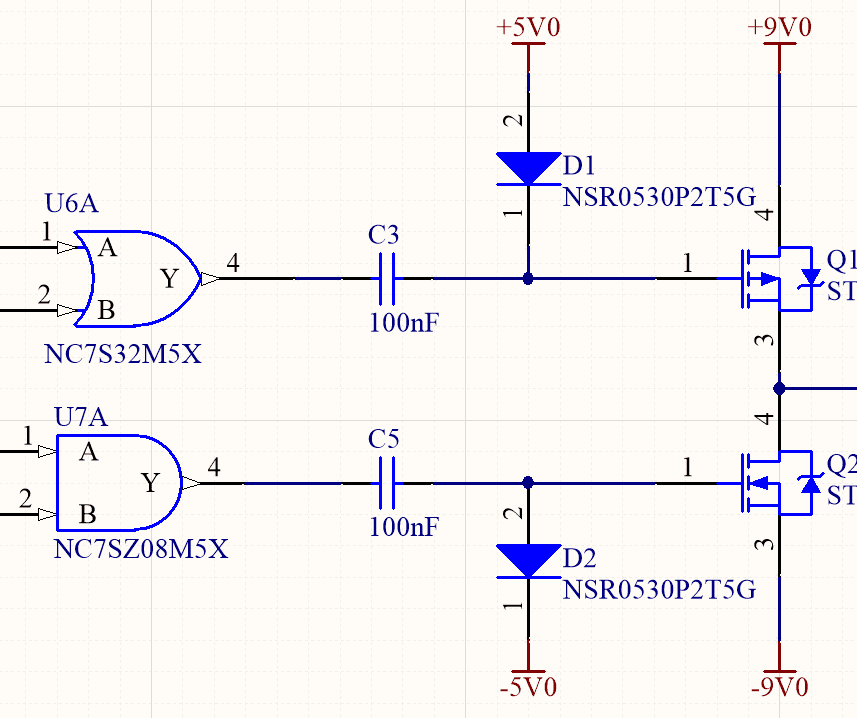
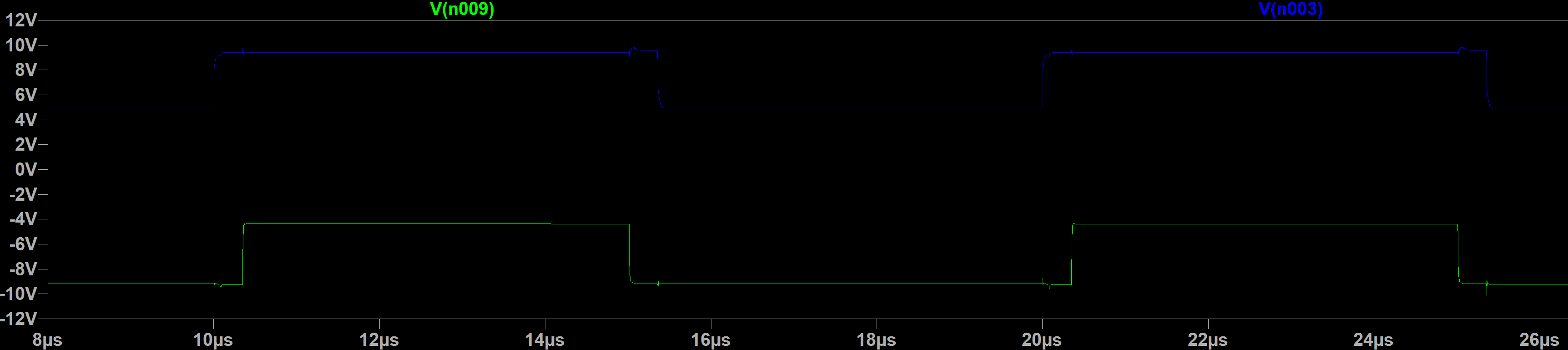
MOSFET 1/2 bridge: The selected switches should have similar switching characteristics.

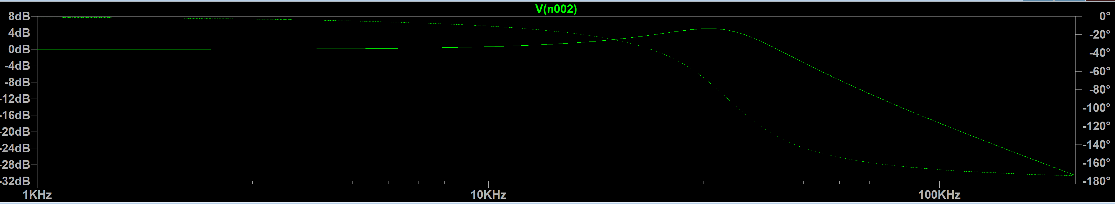
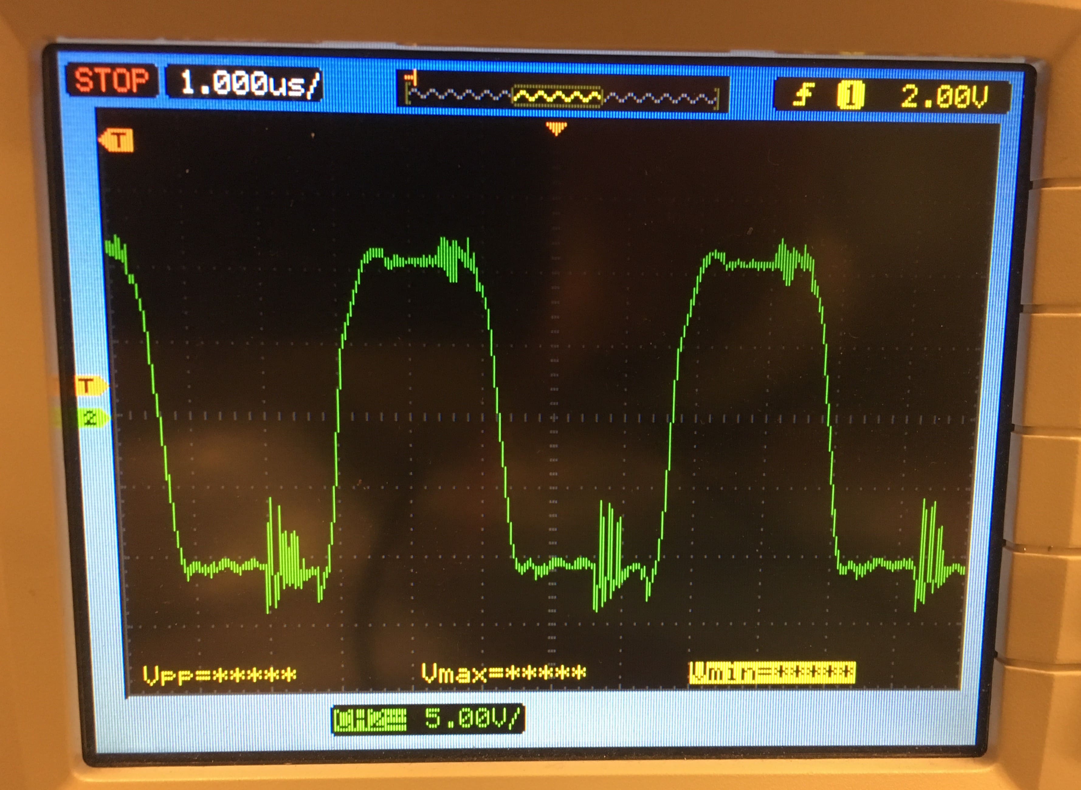
Low Pass Filter: Most class-D amplifiers utilize an LC filter, and the cut-off frequency should be around 30kHz.

—Dead-time Generator

In the half-bridge configuration, if both MOSFETS are on at the same time, a short will be created from V+ to V- (aka shoot-through), which draws a significant amount of current and heats up the MOSFETs.

To avoid this, I designed a circuit to ensure that the pmos does not turn on when the nmos is on. The RC network ensures that the input taken above the capacitor will go HIGH after the input taken above the resistor.

The time constant for this RC network is (1K)(500pF) = 0.5us, which accounts for the propagation delays and rise times for the selected MOSFETs, and is less than the maximum frequency of the square wave (which is 5us).

Green trace = OR gate output, red trace = AND gate output

—Gate Drivers

To drive the gates of the PMOS (high-side driver) and the NMOS (low-side driver), I level-shifted the outputs of the AND gate and the OR gate to properly bias the gate of each MOSFET.

Green trace = NMOS driver, red trace = PMOS driver

—Low Pass Filter

Before driving the speaker, I put the digital encoding of the audio signal through a low pass filter to filter out the high-frequency components and get the analog signal back. I used a cut-off frequency of 35kHz and a passive LC filter.

Since the output of the low-pass filter is the speaker, I took into account the 8 ohm resistance when calculating values for the inductor and capacitor.

—Simulation

Before prototyping the circuit, I downloaded LTSpice models and simulated the second-half of the circuit (from the comparator to the output) to ensure proper functionality.

—Schematic

—Prototype

Before designing the PCB layout, I breadboarded the circuit to tune the deadtime generator circuit and verify circuit functionality.

Green = audio input, Yellow = 200kHz triangle wave
Fixed deadtime insertion
Level shifted NMOS and PMOS gate drivers
Amplified digital signal

—Modifications

After verifying that the board functioned as expected, I started to design the board layout. I decided to power it with a single supply rail, so I had to make some modifications to the circuit. I added in a delay to the turn on time of the NMOS driver so the charge pump capacitor at the gate of the PMOS had time to charge. I also re-biased the gate drivers so the PMOS and NMOS can turn on.

—Board Layout

I designed a 4-layer board that is powered using a USB-C charger. I researched splitting (or partitionign) the analog ground and switching ground, but decided to use one ground reference and keep it clean by having the layer very close (3mil) to the power plane, and using bypass capacitors and bulk capacitors to filter noise and keep the power signals steady (respectively).

I opted for an LDO to get the +5V0 reference voltage for the op-amps and logic gates. I calculated the current draw on the +5V0 plane at 200kHz (the switching frequency), then used the LDO's datasheet to calculate power dissipation. Since the +5V0 line only draws ~5mA, I opted for the cheaper solution. I via-stitched around the regulated voltage to dissipate heat

I also used via stitching to connect the ground planes together (the bottom layer, the second layer, and part of the top layer).

Top Layer
Power Plane

—Takeaways

This project gave me the opportunity to explore analog circuit design and audio amplification and challenged me to come up with new solutions to problems that arose in the design process. The fixed dead-time insertion could also be used in a synchronous buck converter circuit, which could be a fun future exploration.